Highlights from the Research Center
 Electronic Materials
Tokodai Institute for Element Strategy (TIES):
Electronic Materials
Tokodai Institute for Element Strategy (TIES):
Recent Research Progress
- Development of a new p-type transparent amorphous semiconductor utilizing abundant elements
- Elucidation of the role of hydrogen, the most ubiquitous impurity in materials
- Clarification of the key role that hydrogen plays in the degradation of IGZO characteristics
Developing a p-type transparent amorphous semiconductor that can be formed through solution coating
The area of electronic materials targets a vast range of materials using an extremely large number of elements. Today I will talk about some of our more recent representative achievements.
For starters, we developed the first ever p-type transparent amorphous semiconductor that can be synthesized from a liquid phase at room temperature. While research on p-type transparent semiconductors has been ongoing for the past twenty years, our success came by focusing on the three components Cu-Sn-I while modifying the guidelines for materials design. This p-type transparent amorphous semiconductor has electron mobility comparable to that of an n-type amorphous semiconductor typified by IGZO (In-Ga-Zn-O), which is already in practical use to drive pixcels of various flat panel displays.
Since this new semiconductor can easily be deposited on a plastic substrate, there is hope that it can lead to the development of flexible transparent electronic circuits and applications as hole transport layers for OLEDs and perovskite solar cells. This discovery is also relevant to the utilization of abundant elements since Japan is the world’s second largest producer of iodine.
Developing a high-sensitivity TDS system for hydrogen detection
At our research center, we resolved to seek out and study important topics in electronic materials research that have not yet been addressed. One such topic involves hydrogen. The presence of hydrogen is ubiquitous in various materials, but no research project to date has performed full-scale analysis on these materials to determine how hydrogen affects their characteristics.
A hydrogen atom H0 contains a single proton and a single electron. However, isolated hydrogen atoms are extremely rare in nature as the single electron is unstable, rather they ordinarily lose an electron to become a hydrogen ion H+ or gains an electron to become hydride (hydride ion) H–. The chemical shift in nuclear magnetic resonance (NMR) is widely used to evaluate the charge of hydrogen, but chemical shifts do not always have a one-on-one correspondence with charge. Often the chemical shift for H– appears at the same position as OH. Consequently, it seems that the presence of H– may have been overlooked for this reason. Our research has focused on the relationship between hydrogen impurities and the degradation of characteristics in IGZO-TFTs. To begin with, we had to develop a thermal desorption spectroscopy (TDS) system with a detection sensitivity on the order of ppm because conventional apparatuses were not sensitive enough. The principle of TDS is to generate heat and detect the thermally desorbed hydrogen. Therefore, in order to improve sensitivity, we selected materials to prevent the release of gas and produced a system that employs a laser to generate heat and that increases sensitivity while reducing the exhaust velocity.
Assuming that the detection limit of this system has an S/N ratio of 3, the hydrogen detection limit of the system for a thin film sample of 1 cm x 1 cm x 1 µm can be estimated to be 9.5 x 10¹⁵ atoms/cm3. Now it is possible to detect hydrogen concentrations in ZnO and other thin films that were impossible to measure previously, and we look forward to performing much analysis with this system.
Elucidating the role of hydrogen in degrading characteristics of IGZO-TFTs
We began fabricating thin-film transistors (TFT) with IGZO in 2003–04. The technology became practical around 2012, and by 2015 large OLED TVs operating on IGZO-TFTs begin to appear in electronics retail stores. 65-inch 4K displays were released in 2016, yet there are still issues with the technology. Since individual TFTs are provided for switching each pixel, an n-type TFT is almost always in a negative state when constantly illuminated by light. However, the TFTs are difficult to control when the threshold voltage fluctuates.
This was thought to be caused by the band gaps (regions in which electrons cannot be present), but had not been proven through experiments. Therefore, we used secondary ion mass spectrometry (SIMS) to detect hydrogen atoms in the IGZO film and were astounded to discover a hydrogen concentration of 1020 cm-3. This hydrogen presence was confirmed using hard X-ray beam at SPring-8. Therefore, the spectrum of the thin film was extracted to check transmitted and reflected wavelengths. Based on this data, we derived microstructures in the film through simulations and found that H– and, hence, both OH and H–, was present in oxygen-deficient sites.
Next, computations were performed to determine which of OH and H– was causing harm, and the results indicated that H– was a major factor. Measurements using the TDS system mostly proved that H– bonded to metal ions was the origin. The problem is how to remove the H–. Having identified the source of the problem, it is likely that there is some way to resolve it.
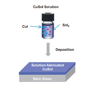
(Caption 1) A p-type amorphous semiconductor Can be fabricated through solution coating or printed at room temperature, and has electron mobility comparable to that of an n-type amorphous semiconductor.
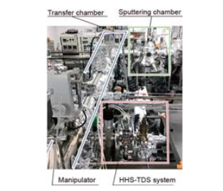
(Caption 2) A prototype high-sensitivity TDS system for detecting hydrogen
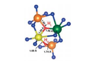
(Caption 3) A structural model of an IGZO thin film. It was demonstrated that H– occupying oxygen-deficient sites was the source of variations in characteristics.
Hideo Hosono, Representative
Tokodai Institute for Element Strategy (TIES)
Tokyo Institute of Technology
Collaborating institutes:
National Institute for Materials Science, High Energy Accelerator Research Organization (KEK), and the University of Tokyo
References:
- [1] T.Hanna et al. Rev. Sci. Instrum. 88, 053103 (2017)
- [2] J.Bang et al. Appl. Phys. Lett. 110, 232105 (2017)
- [3] Y. Hinuma et al. Nat. Commun. 7, 11962 (2016)