 Magnetic materials
Impulsing Paradigm Change through Disruptive Technologies Program (ImPACT)
Material Research for Voltage-Controllable Spintronic Device with Ultralow Energy Consumption and Synchrotron X-ray Spectroscopy to Reveal Interfacial Magnetism- observation

- Computation

-

-

- Developed materials for nonvolatile memory (MRAM) that are effective in reducing power consumption of IT devices
- Elucidated mechanisms of voltage-controlled magnetic anisotropy (VCMA) effect using first-principles calculations and synchrotron radiation at SPring-8
- Discovered a mechanism by which voltage modifies the magnetic dipole TZ term in addition to the orbital magnetic moment
Striving to improve MRAM performance
Power consumption in IT devices could be drastically reduced through development of nonvolatile memory (MRAM) capable of preserving written information without the need for electric power. In consideration for reducing energy required for writing information, spintronic devices employing a magnetic tunnel junction show promise for use in voltage-controlled writing, but their performance must be improved five-to-tenfold current levels to be practical. Accordingly, we conducted research to clarify the mechanisms of the VCMA effect through experiments at SPring-8 and theoretical calculations.
Studying the mechanisms of VCMA using synchrotron radiation
We prepared a device sandwiching a metal magnet having a thickness of a few atomic layers in order to clarify the mechanism of the VCMA effect (Fig. 1). By conducting synchrotron X-ray magnetic circular dichroism at SPring-8 and sum-rule analyses, we are able to evaluate the device’s internal orbital magnetic moment, spin magnetic moment, and magnetic dipole TZ term. Hence, we studied how application of an external voltage changes these physical quantities.
We confirmed that a redox reaction does not trigger changes in magnetic anisotropy in devices with three Fe monolayers and an MgO monolayer. In a device with an interposed ferromagnetic Pt monolayer, we verified from extended X-ray absorption fine structure analysis that the applied voltage does not change the lattice spacing. From these results, we learned that the effects of redox reactions and lattice relaxation were extremely small.
For a device with an inserted monatomic Co layer, we selectively probed only Co to capture changes in the orbital magnetic moment. In a device having FePt and MgO, we similarly probed Pt selectively to capture changes in the magnetic dipole moment TZ term, where the TZ term is a physical quantity produced by an electric quadrupole in the ferromagnet. These findings showed that the mechanisms for VCMA are dominated by the orbital magnetic moment mechanism in 3d-transition metals and is the sum of the orbital magnetic moment mechanism and electric quadrupole mechanism in 5d-transition metals. The involvement of the previously unknown electric quadrupole mechanism was a particularly important discovery (Figure 2).
Contributing to materials development for spintronic devices
Using first-principles calculations to breakdown how each mechanism contributes to VCMA, it was found that the opposite signs of the orbital magnetic moment mechanism and the electrical quadrupole mechanism virtually cancelled each other out, resulting in a small VCMA coefficient of 140 fJ/Vm for the FePt film. In view of the mechanisms of VCMA clarified in this study, we would like to strategically develop materials for spintronics devices having a large VCMA effect.
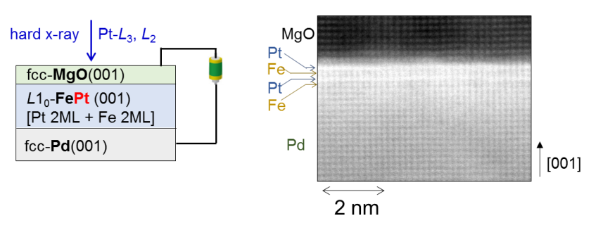
Figure 1 Experimental design employing the world’s largest synchrotron radiation facility SPring-8 TEM cross-sectional image (right) confirms the sample was precisely controlled at the atomic level as intended. Accurate comparisons with first-principles calculations can be made using these high-quality devices.
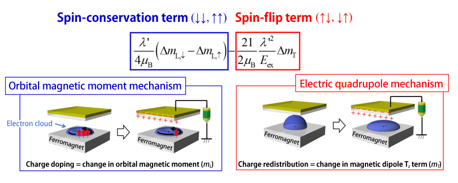
Figure 2 Breaking down VCMA with first-principles calculations VCMA occurs from charge doping (orbital magnetic moment) and redistribution (magnetic dipole TZ term).

Shinji Miwa
Graduate School of Engineering Science
Osaka University
Collaborating institutes:
Y. Suzuki, F. Bonell, K. Matsuda, T. Tsukahara, T. Kawabe, K. Yoshikawa, K. Nawaoka, E. Tamura, and M. Goto of Osaka University; T. Nozaki, and S. Yuasa of AIST; M. Suzuki, T. Nakamura, Y. Kotani, and K. Toyoki of JASRI; M. Tsujikawa, and M. Shirai of Tohoku University; and K. Hono and T. Ohkubo of NIMS
References:
- [1] T. Maruyama et al. ; Nat. Nanotechnol. 4, 158 (2009)
- [2] T. Kawabe et al. ; Phys. Rev. B 96, 220412(R) (2017)
- [3] S. Miwa et al. ; Nat. Commun. 8, 15848 (2017)